#5: Processor: The Software Resolver
A look at what happens in a computer's Central Processing Unit (CPU).

The other day my wife asked me to get a packet of bread. I got ready carrying my wallet and drove down to the shop. Asked the vendor for the bread, swiped the card and back home.
So what, you might say. True! But superficially, this is what a computer processor does. I had no choice but to get the bread stuff.
The act of me getting the bread could be summarized as, executing actions based on an instruction. The instruction is “Get a packet of bread“. To execute this action, I had to perform some actions.
Go to the shop with the intent of buying.
Asked for bread.
Paid amount and completed the transaction.
Returned back home.
All these actions combined get the task completed or executed. A computer processor is no different. The equivalent of each of the actions above is the four phases of processor execution.
Fetch instruction
Decode instruction
Execute instruction
Write back the result
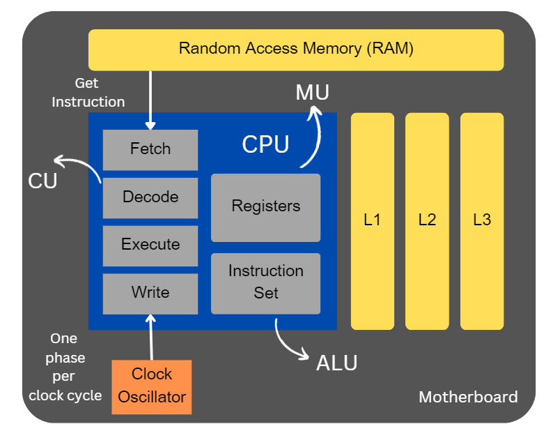
These four phases are the hardware implementations within the processor which make up the Control Unit (CU). The instruction implies the command to the processor which it can understand. The select instructions which a processor supports is called the instruction set.
The code we write gets converted to a collection of instructions to the processor. These instructions post conversion is called the assembly code.
The execution of code we write happens in the order shown below. The instruction set hardware is the hardware implementation specific to an instruction embedded on the processor.
User code → Assembly code → Machine language(0/1) → Instruction set hardware
To get a general sense of how the processor executes, let us say the instruction is to add two numbers 100 and 200.
Add 100 200
At first, this instruction is fetched from the memory into registers on the processor. Registers is the memory in built on the processor for quick access of the instruction. Memory Unit (MU) manages this memory.
Next in the decode phase, this instruction is broken down into its constituent parts. The operator and its operands. In this example its Add and 100, 200 respectively. The address of the registers where the values 100, 200 are stored is also noted down.
Now, the processor is ready to execute the instruction and this is where magic happens. The execute phase has hardware corresponding to the instruction to be executed. The different math instructions supported by the processor is collectively called Arithmetic Logic Unit (ALU). It has electrical components (logic gates) in place to do the computation. The electrical pulses corresponding to binary (0/1) representation of operands 100, 200 are fed into ALU. The resultant 300 an electrical pulse, gets converted to digital form for consumption.
This result is written back to memory and the processor heads on to executing the next instruction.
These four phases are common to any processor. But depending on different processor vendors specialized phases might exist. Right from the point the computer is on, the processor cycles through these four phases. If there are no instructions to execute, the processor is considered idle.
A single processor cycle represents the completion of one phase. This is called Clock Cycle. In our example Add instruction takes four clock cycles to complete its execution.
The number of clock cycles per second is the Clock Speed. For instance, a 3 GHz single processor can run 3 billion clock cycles per second. The Clock Oscillator is the hardware component which generates these clock cycles. This generates clock cycles at certain frequency and it measured in Hertz (Hz). More the clock speed, the faster is the processor.
There are other parameters which govern the performance of a processor. The L1, L2 and L3 cache which reside close to but not on the processor. Not to be confused with registers, which is in built on to the processor. Registers is the fastest memory followed by L1, then by L2 and then L3. These cache units assist the processor for fast data access during execution. What needs to be stored in these cache is decided by the processor. It is not necessary for all L1 to L3 cache to be present. In most cases there will be L1 and L2 cache.
A schematic representation of the component looks as shown below.
All the components here are hardware components and the phases being the hardware operations which act on the instructions produced off of the user code. In the end, the instruction is just an electrical pulse which gets resolved on the ALU.
In short any code we write, either as simple as a calculator or as complex as AI model, the code should get converted to assembly code which the processor can understand. The software layers above are so abstracted that we rarely think of the processor underneath. But, this miniscule piece of technological marvel is the one which gets the stuff done.
Just the way I did for my wife, getting the bread.


